- 您现在的位置:买卖IC网 > Sheet目录17368 > NCP3011GEVB (ON Semiconductor)BOARD EVAL NCP3011 BUCK CTLR
�� �
�
�NCP3011,� NCV3011�
�DETAILED� DESCRIPTION�
�OVERVIEW�
�The� NCP3011� operates� as� a� 400� kHz,� voltage� ?� mode,�
�pulse� ?� width� ?� modulated,� (PWM)� synchronous� buck�
�converter.� It� drives� high� ?� side� and� low� ?� side� N� ?� channel�
�power� MOSFETs.� The� NCP3011� incorporates� an� internal�
�boost� circuit� consisting� of� a� boost� Clamp� and� boost� diode� to�
�provide� supply� voltage� for� the� high� side� MOSFET� Gate�
�driver.� The� NCP3011� also� integrates� several� protection�
�features� including� input� undervoltage� lockout� (UVLO),�
�output� undervoltage� (OUV),� output� overvoltage� (OOV),�
�adjustable� high� ?� side� current� limit� (I� SET� and� I� LIM� ),� and�
�thermal� shutdown� (TSD).� The� NCP3011� includes� a�
�Power� Good� (PG)� open� drain� output� which� flags� out� of�
�regulation� conditions.�
�The� operational� transconductance� amplifier� (OTA)�
�provides� a� high� gain� error� signal� which� is� compared� to� the�
�internal� ramp� signal� using� the� PWM� comparator.� This�
�results� in� a� voltage� mode� PWM� feedback� stage.� The� PWM�
�signal� is� sent� to� the� internal� gate� drivers� to� modulate�
�threshold.� The� device� remains� in� Standby� if� enable� is� not�
�asserted� following� the� 50� m� s� time� period.�
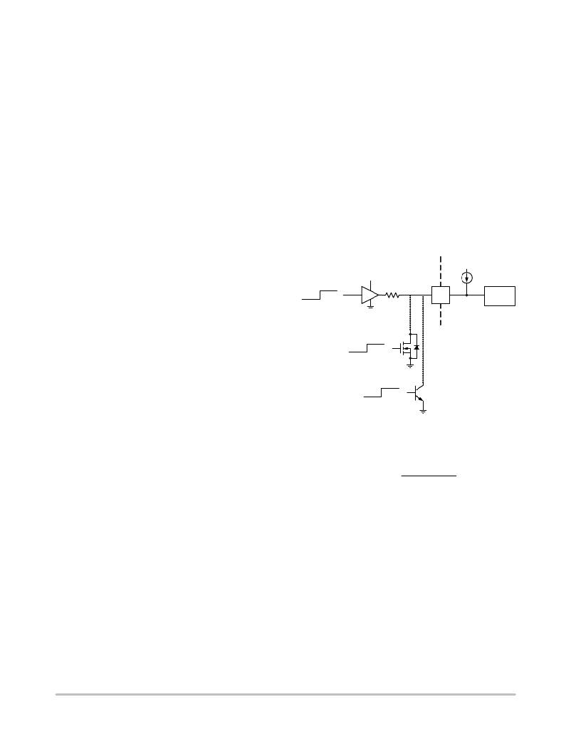
�Enable/Disable�
�The� device� has� an� enable� pin� (EN)� with� internal� 50� m� A�
�pullup� current.� This� gives� the� user� the� option� of� driving� EN�
�with� a� push� ?� pull� or� open� ?� drain/collector� enable� signal.�
�When� driving� EN� with� an� external� logic� supply� a� 10� k� W�
�series� current� limiting� resistor� must� be� placed� in� series� with�
�EN.� See� Figure� 27.� The� maximum� enable� threshold� is� 3.4� V.�
�If� no� external� drive� voltage� is� available,� the� internal� pullup�
�can� be� used� to� enable� the� device,� and� an� open� drain/collector�
�input,� such� as� a� MOSFET� or� BJT� can� be� used� to� disable� the�
�device.� A� capacitor� connected� between� EN� and� ground� can�
�be� used� with� the� internal� pullup� current� source� to� provide� a�
�fixed� delay� to� turn� ?� on� and� turn� off.� See� Equation� 1.�
�V� EN�
�MOSFET� on� and� off� times.� The� gate� driver� stage�
�incorporates� symmetrical� fixed� non� ?� overlap� time� between�
�the� high� ?� side� and� low� ?� side� MOSFET� gate� drives.�
�DISABLE� ENABLE�
�10� k� W�
�EN�
�Enable�
�Logic�
�The� NCP3011� has� a� dual� function� Master/Slave� SYNC�
�pin� In� Slave� mode,� the� NCP3011� synchronizes� to� an� external�
�clock� signal.� In� Master� mode,� the� NCP3011� can� output� a�
�phase� shifted� clock� signal� to� drive� another� master� slave�
�equipped� power� stage� to� provide� a� 180� °� switching�
�relationship� between� the� power� stages.� This� can� help� to�
�?� or� ?�
�ENABLE� DISABLE�
�?� or� ?�
�reduce� the� required� input� filter� capacitance� in� multi� ?� stage�
�power� converters.�
�The� external� 1.25� V� reference� voltage� (VREF)� is�
�provided� for� system� level� use.� It� remains� active� even� when�
�ENABLE�
�DISABLE�
�the� NCP3011� is� disabled.�
�POR� and� UVLO�
�Figure� 27.� Enable� Circuits:� Push� ?� Pull,� Open� ?� Drain,�
�or� Open� ?� Collector�
�C� EN_DLY� +�
�The� device� contains� an� internal� Power� On� Reset� (POR)�
�and� input� Undervoltage� Lockout� (UVLO)� that� inhibits� the�
�internal� logic� and� the� output� stage� from� operating� until� V� CC�
�reaches� their� respective� predefined� voltage� levels.� The�
�internal� logic� takes� approximately� 50� m� s� to� check� the� SYNC�
�pin� and� determine� if� the� device� is� in� Master� mode� or� Slave�
�mode� once� the� voltage� at� V� CC� exceeds� the� rising� UVLO�
�I� PU� T� EN_DLY�
�V� EN_TH�
�C� EN_DLY� =� Delay� Capacitance� (F)�
�I� PU� =� Pullup� Current�
�V� EN_TH� =� Enable� Input� High� Threshold� Voltage�
�T� EN_DLY� =� Desired� Delay� Time�
�(eq.� 1)�
�http://onsemi.com�
�11�
�发布紧急采购,3分钟左右您将得到回复。
相关PDF资料
MIC2505BM
IC SW HIGH SIDE SGL 2A 8SOIC
MIC2505-2BM
IC SW HIGH SIDE SGL 2A 8SOIC
MIC2505-1BM
IC SW HIGH SIDE SGL 2A 8SOIC
TAAB106K020G
CAP TANT 10UF 20V 10% AXIAL
MC34063LBBEVB
EVAL BOARD FOR MC34063LBB
A9BAG-0502F
FLEX CABLE - AFF05G/AF05/AFE05T
EBM08DTMD-S189
CONN EDGECARD 16POS R/A .156 SLD
RCM06DSUI
CONN EDGECARD 12POS DIP .156 SLD
相关代理商/技术参数
NCP3012
制造商:ONSEMI 制造商全称:ON Semiconductor 功能描述:Synchronous PWM Controller
NCP3012DTBR2G
功能描述:电压模式 PWM 控制器 Single Output Buck 0.8V to 40V 70uA RoHS:否 制造商:Texas Instruments 输出端数量:1 拓扑结构:Buck 输出电压:34 V 输出电流: 开关频率: 工作电源电压:4.5 V to 5.5 V 电源电流:600 uA 最大工作温度:+ 125 C 最小工作温度:- 40 C 封装 / 箱体:WSON-8 封装:Reel
NCP301HSN09T1
功能描述:电压监测器/监控器 0.9V Detector RoHS:否 制造商:Texas Instruments 监测电压数:2 监测电压:Adjustable 输出类型:Open Drain 欠电压阈值: 过电压阈值: 准确性:1 % 工作电源电压:1.5 V to 6.5 V 工作电源电流:1.8 uA 最大工作温度:+ 125 C 封装 / 箱体:SON-6 安装风格:SMD/SMT
NCP301HSN09T1G
功能描述:电压监测器/监控器 0.9V Detector w/Reset High RoHS:否 制造商:Texas Instruments 监测电压数:2 监测电压:Adjustable 输出类型:Open Drain 欠电压阈值: 过电压阈值: 准确性:1 % 工作电源电压:1.5 V to 6.5 V 工作电源电流:1.8 uA 最大工作温度:+ 125 C 封装 / 箱体:SON-6 安装风格:SMD/SMT
NCP301HSN10T1
制造商:ONSEMI 制造商全称:ON Semiconductor 功能描述:Voltage Detector Series
NCP301HSN11T1
制造商:ONSEMI 制造商全称:ON Semiconductor 功能描述:Voltage Detector Series
NCP301HSN12T1
制造商:ONSEMI 制造商全称:ON Semiconductor 功能描述:Voltage Detector Series
NCP301HSN13T1
制造商:ONSEMI 制造商全称:ON Semiconductor 功能描述:Voltage Detector Series